Intel High-NA Lithography Update: Dev Work On Intel 18A, Production On Future Node
by Ryan Smith on September 20, 2023 7:20 PM EST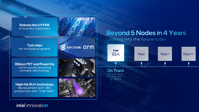
As part of Intel’s suite of hardware announcements at this year’s Intel Innovation 2023 conference, the company offered a brief update on their plans for High-NA EUV machines, which will become a cornerstone of future Intel process nodes. Following some changes in Intel’s process roadmap – in particular Intel 18A being pulled in because it was ahead of schedule – Intel’s plans for the next-generation EUV machines. Intel will now only be using the machines with their 18A node as part of their development and validation work of the new machines; production use of High-NA machines will now come on Intel’s post-18A node.
High Numerical Aperture (High-NA) machines are the next generation of EUV photolithography machines. The massive scanners incorporate 0.55 numerical aperture optics, significantly larger than the 0.33 NA optics used in first-generation production EUV machines, which will ultimately allow for higher/finer quality lines to be etched. Ultimately, High-NA machines are going to be a critical component to enabling nodes below 2nm/20 angstroms.
At the time that Intel laid out their “5 nodes in 4 years” roadmap in 2021, the company announced that they were going to be the lead customer for ASML’s High-NA machines, and would be receiving the first production machine. High-NA, in turn, was slated to be a major part of Intel’s 18A node.
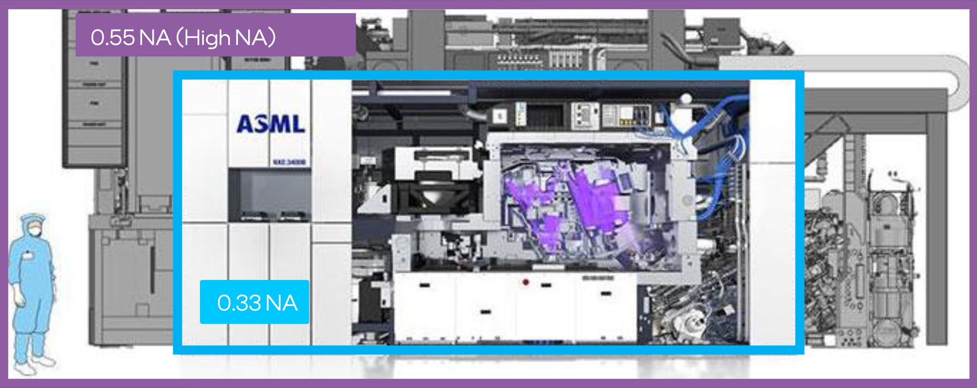
Size Comparison: ASML Normal & High NA EUV Machines
But since 2021, plans have changed for Intel, seemingly in a good way. Progress on 18A has been ahead of schedule, such that, in 2022, Intel announced they were pulling in 18A manufacturing from 2025 to H2’2024. Given that the release date of ASML’s High-NA machines has not changed, however, that announcement from Intel left open some questions about how High-NA would fit into their 18A node. And now we finally have some clarification on the matter from Intel.
High-NA machines are no longer a part of Intel’s production plans for 18A. With the node now arriving before production-grade High-NA machines, Intel will be producing 18A with the tools they have, such as ASML’s NXE 3000 series EUV scanners. Instead, the intersection between 18A and High-NA will be that Intel using the 18A line to develop and validate the use of High-NA scanners for future production. After which, Intel will finally use High-NA machines as part of the production process for their next-generation, post-18A node, which is simply being called “Intel Next” right now.
As for the first High-NA development machine, Intel also confirmed this week that their schedule for development remains on track. Intel is slated to receive their first High-NA machine late this year – which as Pat Gelsinger put it in his keynote, is his Christmas present to Dr. Ann Kelleher, Intel’s EVP and GM of technology development.
Finally, back on the subject of the Intel 18A process, Intel says that they are progressing well on their second-generation angstrom node. The 0.9 PDK, which should be the final pre-production PDK, is nearly done, and should enable Intel’s teams to ramp up designing chips for the process. Intel, for its part, intends to start 18A silicon fab work on Q1’2024. Based on Intel’s roadmaps thus far, that is most likely going to be the first revision of one of the dies on Panther Lake, Intel’s first 18A client platform.


24 Comments
View All Comments
Dante Verizon - Thursday, September 21, 2023 - link
What a strange excess of propaganda in order to show some progress...ballsystemlord - Thursday, September 21, 2023 - link
At least they're not calling it "Intel Superfin eXtreme."name99 - Thursday, September 21, 2023 - link
In other words, if NA-EUV is not being used by 18A, then WHAT is it that defines 18A?Earlier nodes are defined by GAA and BSPD, but 18A without NA-EUV seems a pure marketing node. Or will we see a crazy reach for density that fails, like I10?
dullard - Thursday, September 21, 2023 - link
What is left that has been publicly announced: (1) Ribbon Innovation (whatever that may end up being is not defined) and (2) Line width reduction. That line width reduction could give higher densities or might just be used for a bit less power charging and draining the lines.TristanSDX - Thursday, September 21, 2023 - link
18A is just new name for 20A++stephenbrooks - Thursday, September 21, 2023 - link
These nodes are in pairs I think:4 and 3 are the old 7nm and 7+
20A and 18A are the old 5nm and 5+
In other words, 18A is an "optimisation" node, not a major shake-up.
Wereweeb - Thursday, September 21, 2023 - link
...refinement, obviously. 20A being the jump to GAAFETs, I bet they'll have to use relatively lax tolerances at first, to get it working on a commercial scale. After the experience with 20A, they'll set new goals for feature sizes and work hard on getting there within a commercially viable amount of defects. They can do a lot of work, even without any big updates to their tooling. You know, like all foundries do.This is especially true if their switch to GAAFET isn't going well and they need to be extra lax with tolerances at first to not pull a Samsung and pump out the kind of wafers where instead of finding the defects you search for the rare usable die. Taking it slow and steady is the very opposite approach to the one which led to the Intel 10nm/7 debacle.
AJL - Thursday, September 21, 2023 - link
So, which Fab will be ready in 2024 to ramp up 18A?Ryan Smith - Thursday, September 21, 2023 - link
It'll be Oregon first, as always. Since they need an 18A line to play with the High-NA machine, it'll be D1X, which was specifically upgraded earlier in the decade to house those machines. (They're 3 stories tall!)https://www.anandtech.com/show/17344/intel-opens-d...
AJL - Friday, September 22, 2023 - link
Thanks Ryan! I probably read that article back then, but the old grey matter isn't what it used to be ;-)