AMD Zen 3 Ryzen Deep Dive Review: 5950X, 5900X, 5800X and 5600X Tested
by Dr. Ian Cutress on November 5, 2020 9:01 AM ESTSection by Andrei Frumusanu
The New Zen 3 Core: High-Level
As we dive into the Zen3 microarchitecture, AMD made a note of their journey of the last couple of years, a success-story that’s been started off in 2017 with the revolutionary Zen architecture that helped bring AMD back to the competitive landscape after several sombre years of ailing products.
The original Zen architecture brought a massive 52% IPC uplift thanks to a new clean-sheet microarchitecture which brought at lot of new features to the table for AMD, introducing features such as a µOP cache and SMT for the first time into the company’s designs, as well as introducing the notion of CPU core-complexes with large (8MB at the time) L3 caches. Features on a 14nm FinFET process node, it was the culmination and the start-off point of a new roadmap of microarchitectures which leads into today’s Zen3 design.
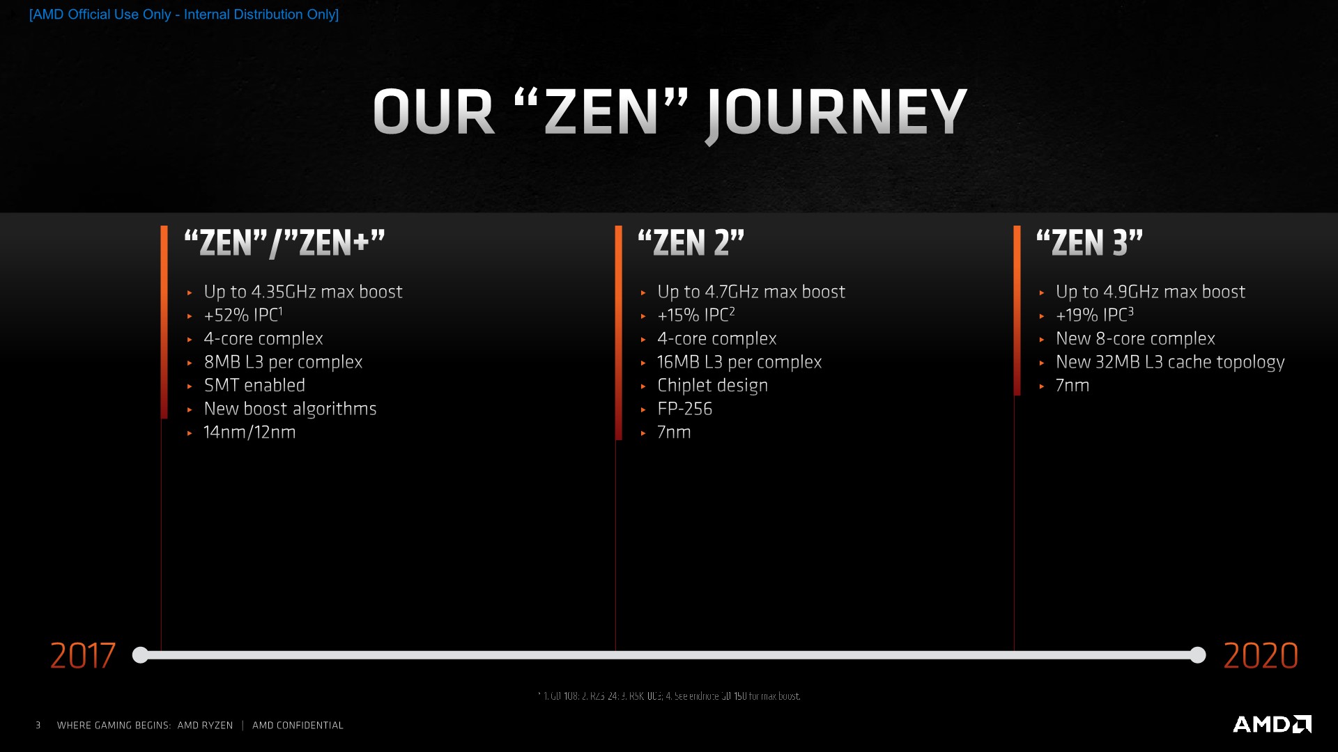
Following a minor refresh in the form of Zen+, last year’s 2019 Zen2 microarchitecture was deployed into the Ryzen 3000 products, which furthered AMD’s success in the competitive landscape. Zen2 was what AMD calls a derivative of the original Zen designs, however it contained historically more changes than what you’d expect from such a design, bringing more IPC increases than what you’d typically see. AMD saw Zen2 as a follow-up to what they had learned with the original Zen microarchitecture, fixing and rolling out design goal changes that they had initially intended for the first design, but weren’t able to deploy in time for the planned product launch window. AMD also stated that it enabled an opportunity to bring some of the future Zen3 specific changes were moved forward into the Zen2 design.
This was also the point at which AMD moved to the new chiplet design, leveraging the transition to TSMC’s new 7nm process node to increase the transistor budget for things like doubling the L3 cache size, increasing clock speeds, and vastly reducing the power consumption of the product to enable aggressive ramp in total core counts both in the consumer space (16-core Ryzen 9 3950X), as well as in the enterprise space (64-core EPYC2 Rome).
Tying a cutting-edge high-performance 7nm core-complex-die (CCD) with a lower cost 12/14nm I/O die (IOD) in such a heterogenous package allowed AMD to maximise the advantages and minimise the disadvantages of both respective technologies – all whilst AMD’s main competitor, Intel, was, and still is, struggling to bring out 10nm products to the market. It was a technological gamble that AMD many times has said was made years in advance, and has since paid off plenty.
Zen 3 At A Glance
This brings us to today’s Zen3 microarchitecture and the new Ryzen 5000 series. As noted earlier, Mark Papermaster had mentioned that if you were to actually look at the new design from a 100,000-foot level, you’d notice that it does look extremely similar to previous generation Zen microarchitectures. In truth, while Zen3 does share similarities to its predecessors, AMD’s architects started off with a clean-sheet design, or as they call it – “a ground-up redesign”. This is actually quite a large claim as this is a quite enormous endeavour to venture in for any company. Arm’s Cortex-A76 is the most recent other industry design that is said to have been designed from scratch, leveraging years of learning of the different design teams and solving inherent issues that require more invasive and large changes to the design.
Because the new Zen3 core still exhibits quite a few defining characteristics of the previous generation designs, I think that AMD’s take on a “complete redesign” is more akin to a deconstruction and reconstruction of the core’s building blocks, much like you’d dismantle a LEGO set and rebuild it anew. In this case, Zen3 seems to be a set-piece both with new building blocks, but also leveraging set pieces and RTL that they’ve used before in Zen2.
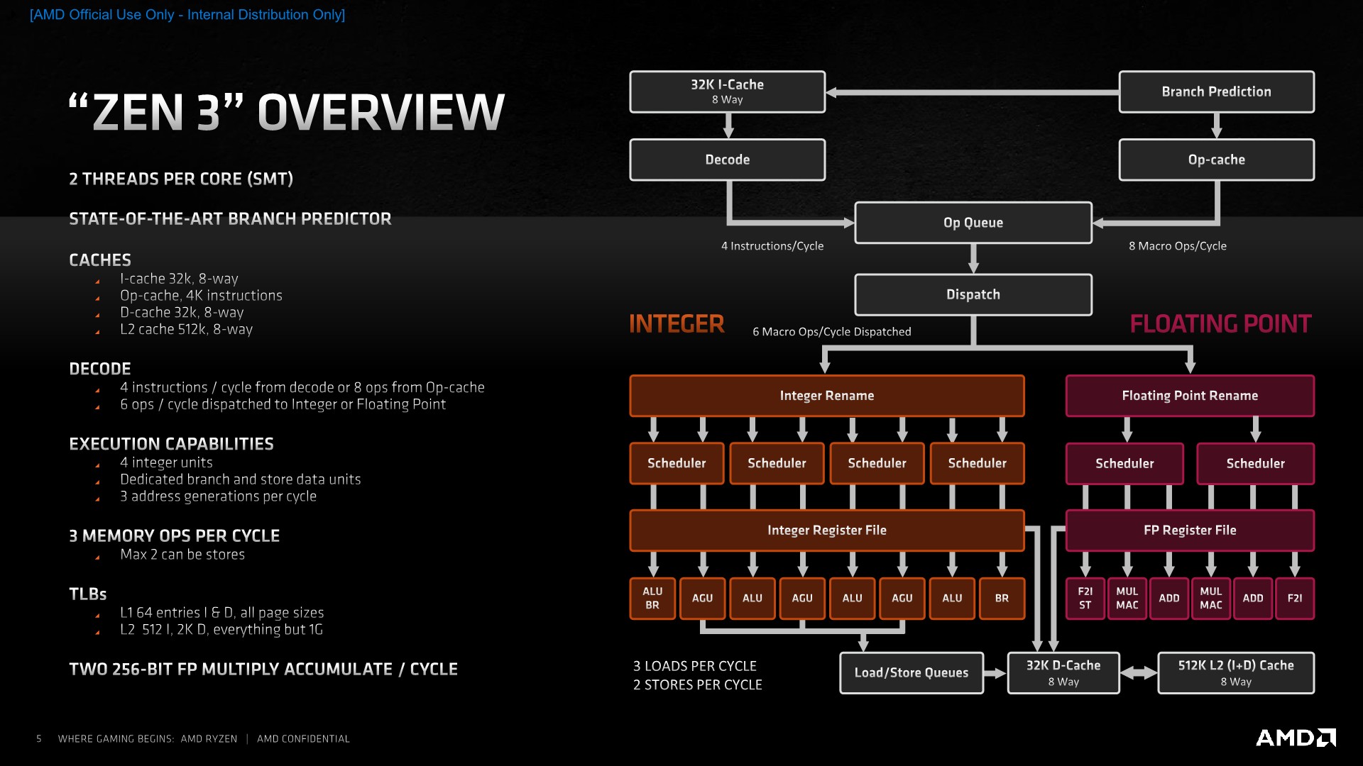
Whatever the interpretation of a “clean-sheet” or “complete redesign” might be, the important take is that Zen3 is a major overhaul in terms of its complete microarchitecture, with AMD paying attention to every piece of the puzzle and trying to bring balance to the whole resulting end-design, which comes in contrast to a more traditional “derivative design” which might only touch and see changes in a couple of the microarchitecture’s building blocks.

AMD’s main design goals for Zen3 hovered around three main points:
- Delivering another significant generational single-threaded performance increase. AMD did not want to be relegated to top performance only in scenarios where workloads would be spread across all the cores. The company wanted to catch up and be an undisputed leader in this area to be able to claim an uncontested position in the market.
- Latency improvements, both in terms of memory latency, achieved through a reduction in effective memory latency through more cache-hits thanks to the doubled 32MB L3 that an individual core can take advantage of, as well as core-to-core latency which again thanks to the consolidated single L3 cache on the die is able to reduce long travel times across the dies.
- Continuing a power efficiency leadership: Although the new Zen3 cores still use the same base N7 process node from TSMC (although with incremental design improvements), AMD had a constraint of not increasing power consumption for the platform. This means that any new performance increases would have to come through simultaneous power efficiency improvements of the microarchitecture.
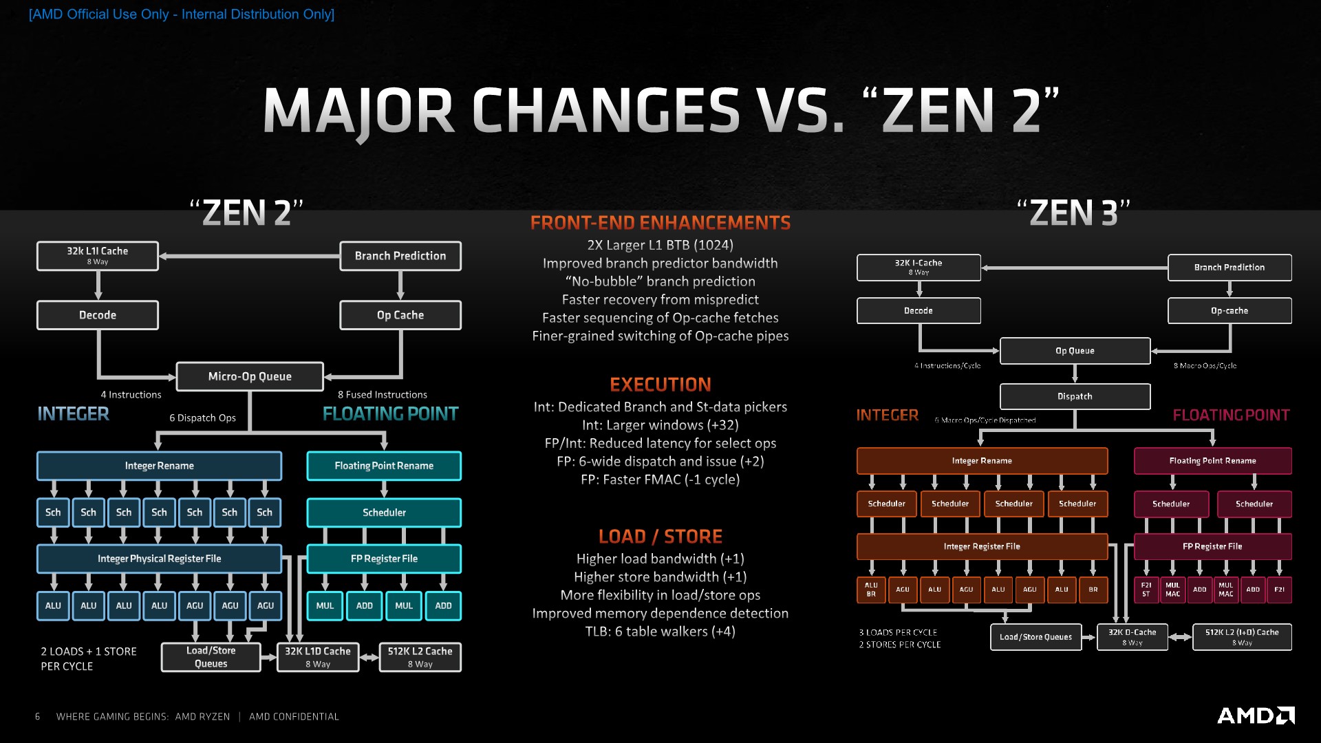
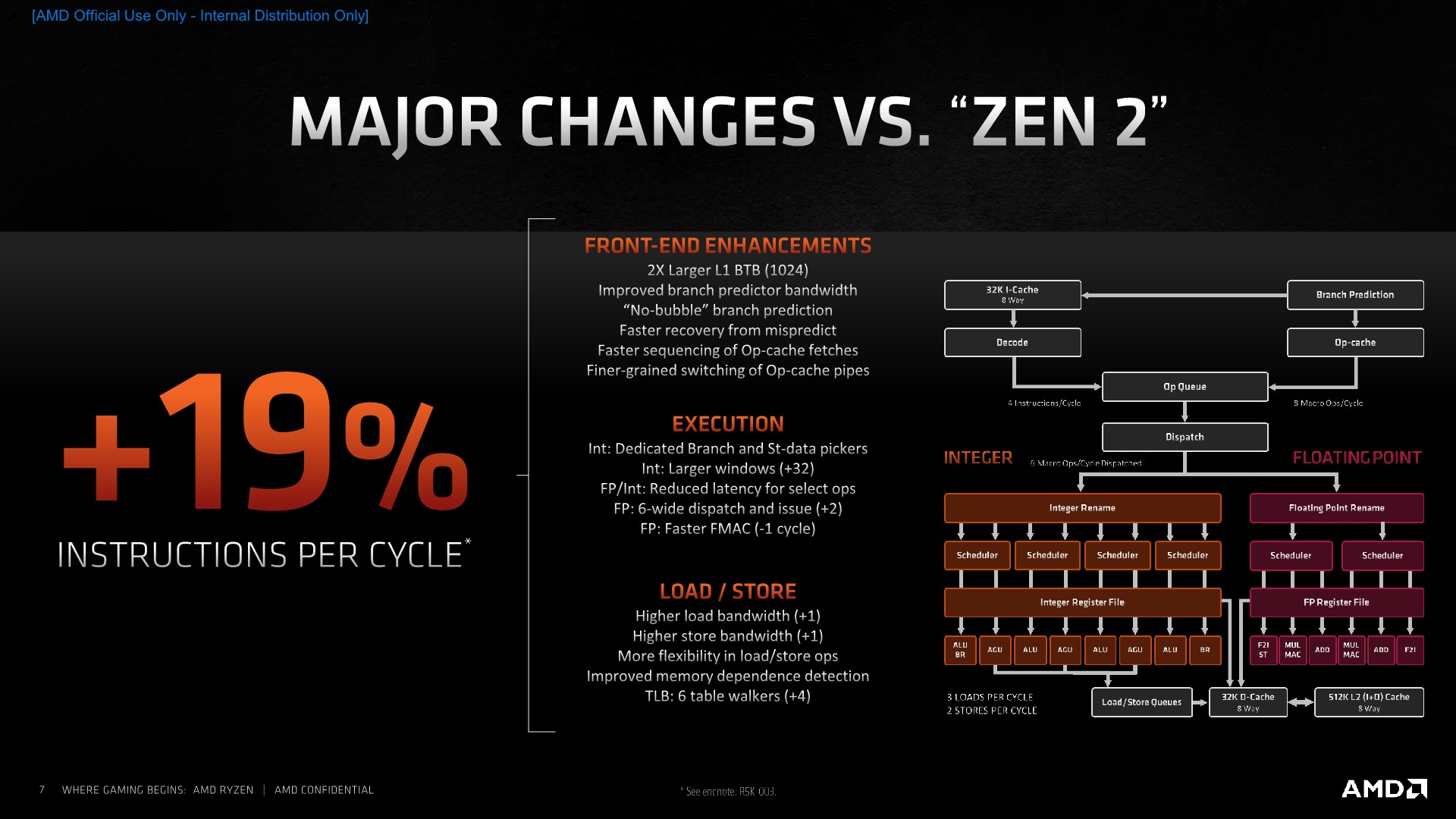
The culmination of all the design changes AMD has made with the Zen3 micro-architecture results in what the company claims as a 19% average performance uplift over a variety of workloads. We’ll be breaking down this number further into the review, but internal figures show we are matching the 19% average uplift across all SPEC workloads, with a median figure of 21%. That is indeed a tremendous achievement, considering the fact that the new Ryzen 5000 chips clock slightly higher than their predecessors, further amplifying the total performance increase of the new design.


339 Comments
View All Comments
Jvanderlinde - Saturday, November 7, 2020 - link
Glad to read the 2700x is taken into account. The 5950X seems like a hell of an upgrade coming from that path. Gotta love AMD for what it's bin accomplishing in the last few years.Kallan007 - Saturday, November 7, 2020 - link
I just want to thank AMD for a lovely way to end 2020! I cannot wait for those AMD 6000 series card reviews! Good job as always AnandTech!Pumpkinhead - Saturday, November 7, 2020 - link
How is that possible that peak power for the 3700x having 8 cores is lower than for 3600 with 6 cores?nandnandnand - Saturday, November 7, 2020 - link
"Compared to other processors, for peak power, we report the highest loaded value observed from any of our benchmark tests."They selected the highest single wattage value from ANY of their tests. So at the same TDP, they should be very close to each other. I guess the point is to find the worst case scenario for each processor, rather than an average, to determine the power supply needed. Other reviews point to 3600 using less power on average:
https://www.tomshardware.com/reviews/amd-ryzen-5-3...
Pumpkinhead - Saturday, November 7, 2020 - link
>https://www.tomshardware.com/reviews/amd-ryzen-5-3...Interesting that 3700x being 1/3 faster in handbrake still draws only 13% more power, I always thought that in parallel workloads it power consumption scales linearly as you add more cores.
Even tho in AIDA stress test it draws 35% more power so peak consumption is different too, also look at the 5800x - draws almost twice as 5600x (also 6c vs 8c)
Kjella - Sunday, November 8, 2020 - link
It scales linearly until you hit the TDP, past that more cores lets you use a lower, more efficient frequency. As long as you can keep all cores loaded 8 cores on a 10W/core power budget will get less done than 16 cores at a 5W/core power budget even though 8*10 = 16*5. But with disabled cores you might have to run more of the chip, like the whole CCX to support 3 of 4 working cores. That will obviously be less efficient since the "overhead" has to be split by 3 instead of 4.Murilo - Saturday, November 7, 2020 - link
..and AMD price? ahahah.I want price!
psyclist80 - Saturday, November 7, 2020 - link
Im glad you guys added in Tiger Lake...very important data point. If it beat willow cove in its full implementation then its certainly going to beat the watered down 14nm version cypress cove and slay it on power efficiency.Im glad AMD has taken the crown back (last held 2003-2006)...as has been said in the past, the Empire will strike back...Hopefully Golden Cove can do that for Intel. That will face 5nm Zen 4 though...AMD looking strong for the next year or two!
Sushisamurai - Sunday, November 8, 2020 - link
apparently, looking at other reviews, there appears to be a performance uplift/downgrade (depends how you look at it) with the number of RAM sticks populated on the board (2 vs 4). I wonder how much of a difference it is with RAM speeds and memory stick population on the 5000 series.umano - Sunday, November 8, 2020 - link
I bought in june a 3800x and an x570 creator planning to upgrade to 5950x after zen 4 launches, but often, when we have more power, we find a way to crave for more. I work in fashion ph, for me the 35% bump in ps compared to my 3800x (bought because the price was the same as 3700) is a no brainer. It will also help me in capture one exports and zip compression. I did not think an upgrade so soon will benefit me so much, but you know life happens. Good job amd you made technology fun again