New Intel CEO Making Waves: Rehiring Retired CPU Architects
by Dr. Ian Cutress on January 21, 2021 5:05 AM EST- Posted in
- CPUs
- Intel
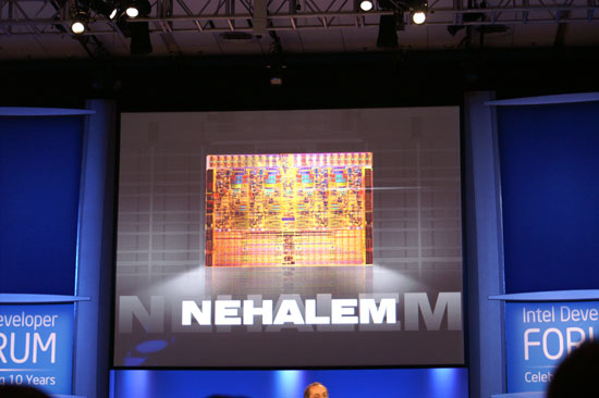
- Nehalem
- Pat Gelsinger
We’re following the state of play with Intel’s new CEO, Pat Gelsinger, very closely. Even as an Intel employee for 30 years, rising to the rank of CTO, then taking 12 years away from the company, his arrival has been met with praise across the spectrum given his background and previous successes. He isn’t even set to take his new role until February 15th, however his return is already causing a stir with Intel’s current R&D teams.
News in the last 24 hours, based on public statements, states that former Intel Senior Fellow Glenn Hinton, who lists being the lead architect of Intel’s Nehalem CPU core in his list of achievements, is coming out of retirement to re-join the company. (The other lead architect of Nehalem are Ronak Singhal and Per Hammerlund - Ronak is still at Intel, working on next-gen processors, while Per has been at Apple for five years.)
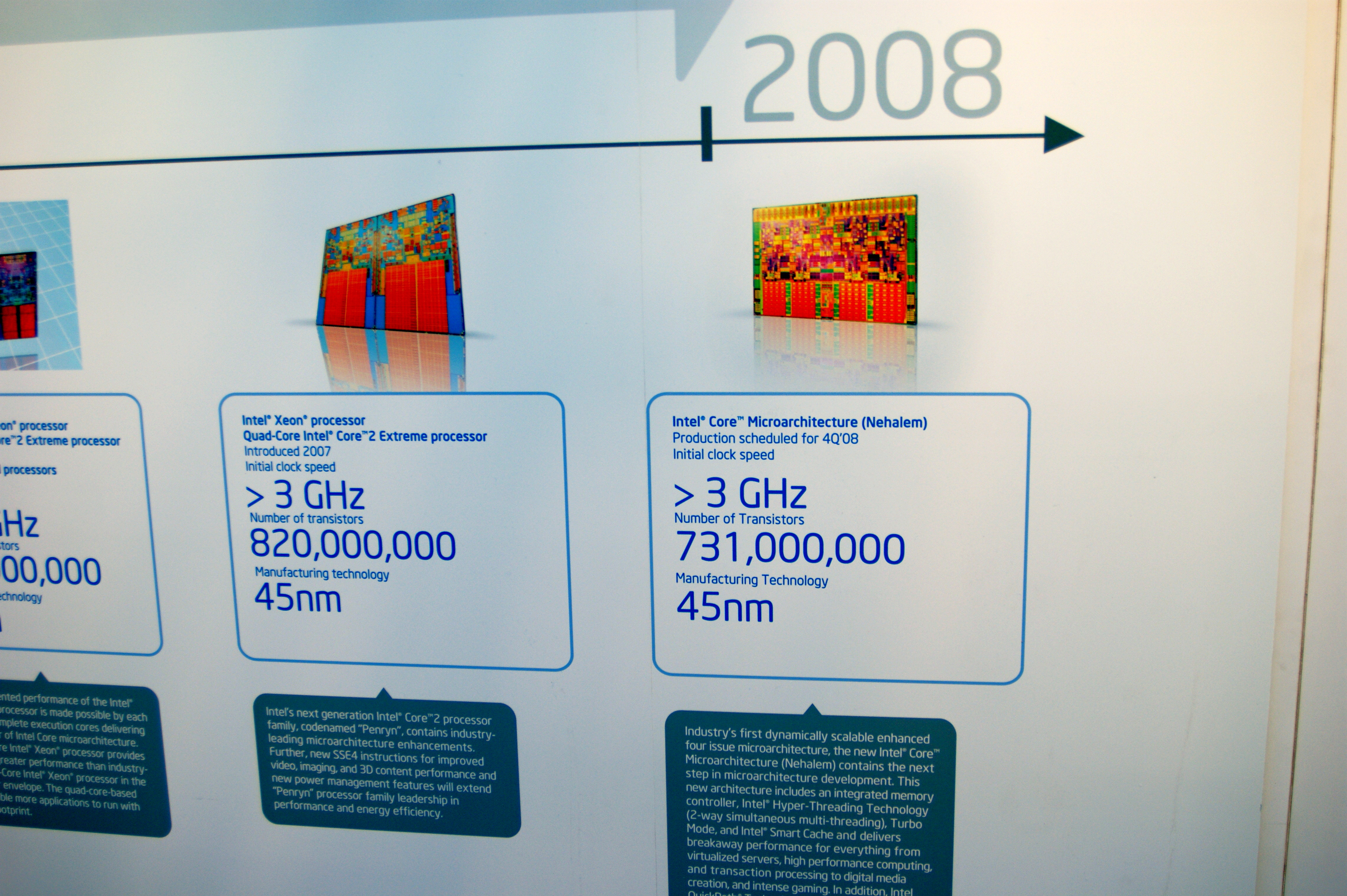
Hinton is an old Intel hand, with 35 years of experience, leading microarchitecture development of Pentium 4, one of three senior architects of Intel’s P6 processor design (which led to Pentium Pro, P2, P3), and ultimately one of the drivers to Intel’s Core architecture which is still at the forefront of Intel’s portfolio today. He also a lead microarchitect for Intel’s i960 CA, the world’s first super-scalar microprocessor. Hinton holds more than 90+ patents from 8 CPU designs from his endeavors. Hinton spent another 10+ years at Intel after Nehalem, but Nehalem is listed in many places as his primary public achievement at Intel.

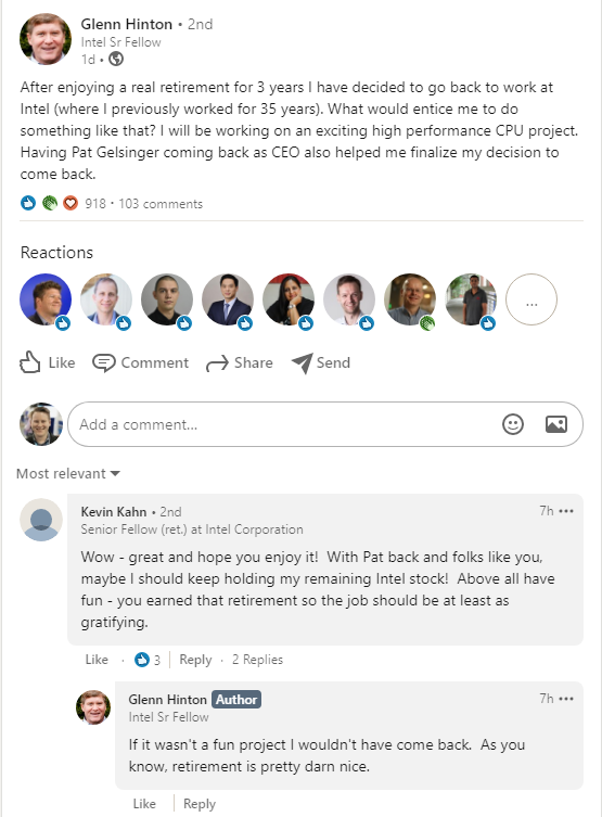
On his social media posts, Hinton states that he will be working on ‘an exciting high performance CPU project’. In the associated comments also states that ‘if it wasn’t a fun project I wouldn’t have come back – as you know, retirement is pretty darn nice’. Glenn also discloses that he has been pondering the move since November, and Gelsinger’s re-hiring helped finalize that decision. His peers also opine that Glenn is probably not the only ex-Intel architect that might be heading back to the company. We know a few architects and specialists that have left Intel in recent years to join Intel's competitors, such as AMD and Apple.
There are a few key things to note here worth considering.
First is that coming out of retirement for a big CPU project isn’t a trivial thing, especially for an Intel Senior Fellow. Given Intel’s successes, one would assume that the financial situation is not the main driver here, but the opportunity to work on something new and exciting. Plus, these sorts of projects take years of development, at least three, and thus Glenn is signing on for a long term despite already having left to retire.
Second point is reiterating that last line – whatever project Glenn is working on, it will be a long term project. Assuming that Glenn is talking about a fresh project within Intel’s R&D ecosystem, it will be 3-5 years before we see the fruits of the labor, which also means creating a design aimed at what could be a variety of process node technologies. Glenn’s expertise as lead architect is quite likely applicable for any stage of an Intel R&D design window, but is perhaps best served from the initial stages. The way Glenn seems to put it, this might be a black-ops style design. It also doesn't specify if this is x86, leaving that door open to speculation.
Third here is to recognize that Intel has a number of processor design teams in-house and despite the manufacturing process delays, they haven’t been idle. We’ve been seeing refresh after refresh of Skylake lead Intel's portfolio, and while the first iterations of the 10nm Cove cores come to market, Intel’s internal design teams would have been working on the next generation, and the next generation after that – the only barrier to deployment would have been manufacturing. I recall a discussion with Intel’s engineers around Kaby Lake time, when I asked about Intel’s progress on IPC – I requested a +10% gen-on-gen increase over the next two years at the time, and I was told that those designs were done and baked – they were already working on the ones beyond that. Those designs were likely Ice/Tiger Lake, and so Intel’s core design teams have been surging ahead despite manufacturing issues, and I wonder if there’s now a 3-4 year (or more) delay on some of these designs. If Glenn is hinting at a project beyond that, then we could be waiting even longer.
Fourth and finally, one of the critical elements listed by a number of analysts on the announcement of Gelsinger’s arrival was that he wouldn’t have much of an effect until 3+ years down the line, because of how product cycles work. I rejected that premise outright, stating that Pat can come in and change elements of Intel’s culture immediately, and could sit in the room with the relevant engineers and discuss product design on a level that Bob Swan cannot. Pat has the opportunity to arrange the leadership structure and instill new confidence in those structures, some of which may have caused key architects in the past to retire, instead of build on exciting projects.
As we can see, Pat is already having an effect before his name is even on the door at HQ.
Today is also Intel’s end-of-year financial disclosure, at 5pm ET. We are expecting Intel’s current CEO, Bob Swan, to talk through what looks to be another record breaking year of revenue, and likely the state of play for Intel's own 7nm process node technologies. That last point is somewhat thrown into doubt given the new CEO announcement and if Gelsinger is on the call. It is unknown if Gelsinger will participate.
Related Reading
- Intel Appoints Pat Gelsinger as New CEO, From Feb 15th
- An Interview with Intel CEO Bob Swan: Roundtable Q&A on Fabs and Future
- Robert Swan Named CEO of Intel


112 Comments
View All Comments
GeoffreyA - Friday, January 22, 2021 - link
It's possible the P4 would've gone on a bit more if Northwood had been widened and its stages cut down. But Intel was still under the deep-pipeline/MHz delusion back then, which led to Prescott, whose 31 stages were supposed to usher in 10 GHz. Today's CPUs---Sandy Bridge and upwards, and Zen---have up to 19 stages, pretty close to the P4's 20. The difference is they're much wider, among other things (bigger caches, better branch prediction,* effective micro-op cache, etc.).* In that era, the Pentium 4's branch prediction was superior to the K8's, but the latter wasn't being handicapped by a lengthy pipeline. Prescott improved on this further, adding the Pentium M's indirect prediction. But all that couldn't overcome the deep pipeline.
mode_13h - Saturday, January 23, 2021 - link
Wasn't Prescott forced to deepen its pipelines in order to cope with 64-bit (which ended up not really being enabled until the Pentium D)?By the time Prescott was designed, I think Intel was well aware that P4 would never come close to 10 GHz. Scaling to 10 GHz was just an initial design goal of the NetBurst uArch, and badly underestimated leakage of the target process nodes is ultimately what sabotaged it. If manufacturing had managed to deliver on that front, then the NetBurst uArch could have upheld its part in enabling those frequencies.
GeoffreyA - Sunday, January 24, 2021 - link
I believe it was due to clock speed mainly, more stages allowing each to be simpler and so clock higher. The idea was that Prescott would carry on Willamette and Northwood's philosophy, adding another 11, just like they added 10 to the Pentium III. Any loss in IPC would be offset by frequency. Unfortunately, it reached only 3.8 GHz and took a lot of power to do so. I remember the Pentium Ds felt terribly slow in Windows too, compared to Willamette and Northwood.As for x64, I reckon it wasn't that difficult to add. Just widening and adding of registers I believe, along with some other changes.
GeoffreyA - Sunday, January 24, 2021 - link
On a side note, people might wonder how could Intel have been so stupid to come up with Prescott. I think it's rather that Prescott's design was laid down long before it became apparent what a blunder Netburst was, with its deep-pipeline/high MHz/low IPC principle.mode_13h - Sunday, January 24, 2021 - link
> I think it's rather that Prescott's design was laid down long before it became apparent what a blunder Netburst wasMaybe they still thought they could get leakage under control, which would've really let it stretch its legs. People have clocked Prescotts above 6 GHz with LN2 cooling, which shows they were still thinking high clockspeeds were a viable option, as it was being designed.
GeoffreyA - Sunday, January 24, 2021 - link
I remember that Cedar Mill (Prescott's last revision) curtailed power quite a bit, or brought down the TDP to 65W. I need to read up about CM. Curious to see what they did. Don't think it was a die shrink.mode_13h - Monday, January 25, 2021 - link
> Don't think it was a die shrink.It was, for sure. I remember reading about one last die shrink and was eager to see how it would stack up against Core 2, when they were on the same process node. IIRC, the results were still pretty disappointing for the P4. However, I didn't pay much/any attention to perf/W, which it sounds like was the main improvement.
GeoffreyA - Tuesday, January 26, 2021 - link
"one last die shrink"You're quite right. It was the 65 nm node.
https://www.anandtech.com/show/1834/2
mode_13h - Sunday, January 24, 2021 - link
> I believe it was due to clock speed mainly, more stages allowing each to be simpler and so clock higher.It's true that Prescott did clock higher than Northwood.
> As for x64, I reckon it wasn't that difficult to add. Just widening and adding of registers I believe, along with some other changes.
It also adds more registers, which means widening muxes. More importantly, 64-bit arithmetic increases the critical path, because each bit in result is contributed to by the lower-order bits. Therefore, I wonder if they had to reduce the complexity of some pipeline stages, when going to 64-bit, which would have to be compensated for by adding more of them.
GeoffreyA - Sunday, January 24, 2021 - link
Likely, they used every opportunity available to squeeze 31 stages out of Northwood's 20. How much of a hand 64-bit had in that, I can't say, but doubt whether it was a massive role. Looking at the K8, it had only two more stages than K7's 10. And Core, at 14, was roughly the same as the Pentium M.